

Solid-State Rectifier Testing, Part 2

[August 2014] Previously, Gary Minker discussed how technicians could better understand rectifiers and how to troubleshoot them in circuits. By putting that knowledge to work with the right test gear, it is possible to save time, money and lost airtime. Now, Gary puts it all together.
Unless your technical abilities are limited to swapping modules, eventually you will find yourself troubleshooting a piece of gear where you will need to know if the solid-state rectifiers are working correctly.
Fortunately, testing rectifiers is not rocket science. All you need for most situations is some basic equipment and a little common sense. Indeed, as we shall see, while digital and analog meters are helpful, the old Lissajou trace still reigns supreme.
Small Silicons
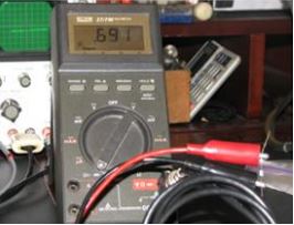
Fortunately, reliable testing of most garden variety silicon devices is easily accomplished via the diode test function on many of the newer digital Volt meters.
The resulting voltage display is a true representation of the forward breakdown conduction voltage of the junction in the device under test.
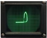
At the same time, a quick look at the junction on a curve tracer will give very reliable Go/No Go indications. The sharp, almost 90 degree, “knee” at the point of conduction in a standalone or small silicon device shows the nonlinear action of the junction. Here are a couple of screen shots to demonstrate:
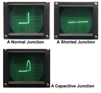
Using this system requires no mathematics. The picture tells the story. In fact, any visual anomalies that cannot be explained on the curve tracer should flag the device under test.
Zener Diodes
Zener devices on the other hand may not be tested as easily.
While the diode test function will give an indication of the one junction, and the Lissajous trace will show the forward conduction, unless the tracer is capable of generating the known reverse conduction voltage, this diode will go improperly tested, especially when you might be looking for a generic replacement without going by the data sheet numbers.
Furthermore, errantly installing a Zener diode in place of a normal junction device will cause additional damage to an already defective circuit. Any time you have a Zener as the known or suspect device under test, the forward bias conduction point should be examined in one-tenth Volt increments for ratings under 30 Volts. Zeners over this voltage are typically not set up for critical tolerance device under test, and may be tested more liberally in one Volt increments.
In either test, the Zener should not show any appreciable current flow until the actual “knee” is reached, at which point the junction will cave in, and current will rise very quickly.
Additionally, remember to be cautious when reverse bias testing Zener devices to insure that the dissipation limit of the device under test is not exceeded.
Large Silicons
Testing of high voltage and high current silicons can require a very different scenario.
Silicons which handle voltages of up to 1,000 Volts or so and currents of up to 100 Amperes or so will react to most usual junction tests. Diode junction tests and Lissajous traces will show most anomalies in these devices. Stressing these large units up to the PIV (Peak Inverse Voltage) mode often will show any potential problems within the device. And reverse bias capacitance test comparisons may point out partially open devices when compared to the previously established look up charts.
However, silicons which handle voltages in excess of 2 kV do not respond in the usual ways.
First, in high voltage devices the forward conduction breakdown voltage is often greater than most digital meter diode test functions will provide, thus rendering this meter’s test function useless. While standard curve tracers may give some valid indication of the condition of the numerous individual junctions strung in series within the device under test, this generally good optical view is only cursory at best.
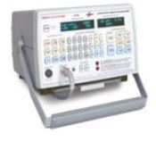
These devices now require the talents of the more specialized and adaptive test instruments, such as the Sencore LC-103 (Shown below).
Visual Clues
Small form, high voltage devices typically are epoxy potted in order to keep the internal diodes in physical check. Failure is often typified by an obvious burn mark or crack on the exterior surface.
Should this not be the case, test first for forward conduction by developing lookup chart data voltage in the terminals and comparing results. A device partially shorted – either by non-visible carbonization of the internal case or by a number of shorted diodes within the string – will show a definitely lower forward conduction threshold along with a correspondingly higher forward milliamperage flow at a given voltage. Partially shorted units will show good reverse milliamperage leakage but will generally fail the PIV and capacitance comparison tests.
Large mono block silicons are seldom equalized internally, but additional tests for capacitance will help to ferret out additional problems in these units. Comparison of a suspect device under test to the previously completed lookup charts will give a reliable indication as to the condition of the suspect device.
Stacked or Composite Silicons
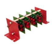
The most common high voltage rectifier is an item of very creative electromechanical art. These large physical structures often weighing several pounds are designed to accommodate many purposes.
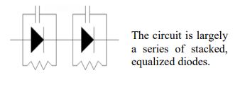
Great use of air and fiberboard dielectric facilitates not only inter-component electrical insulation but cooling by forced clean air as well. Many of these large structures are repairable. Damaged components are simply removed and replaced with tested new parts. The basic structure of the stacked diode array consists of:
- The support form. Always an insulative material of very high dielectric strength.
- Diode support structure. Often conductive and serves as a heat sink to dissipate destructive thermal energy.
- Equalizing resistors. These resistors are placed in parallel electrically with each diode to optimize or “equalize” any sudden imbalance within the stack.
- Transient (snubber) capacitors. These capacitors are placed in parallel electrically with each diode and serve to absorb any possibly damaging spikes which may appear in the stack.
For example, this stack or composite of components is very complex to test. The device pictured consists of twenty type 1N3495 diodes.
The circuit is largely a series of stacked, equalized diodes.
Press Fit Silicon Devices
The 1N3495 is a 400 Volt, 25 Ampere cathode case device.
From this information quite a bit may be surmised about the stress limits and testing criteria of this stack. In fact, absolutely nothing needs to be known about the machine or transmitter in which this stack is operated. Of course, ancillary information is possibly helpful in understanding why this stack failed, but strictly from a test and quality assurance point, the diode information is all that is required.
With a 1,000 Volt rating on each equalizing capacitor noted, the information gathering is complete and testing may begin. As each diode is of the small silicon class, and no further information supports deviation, each diode may be tested first with the diode function feature of the digital meter.
Diode Test Meter Function
Forward bias testing shows each forward voltage drop to be in the nominal .51 Volt range. Reverse bias testing will show over-range which confirms the preliminary health of the diode. Switching the digital meter to an Ohms scale will show the nominal value of the equalizing resistor to be 25,000 Ohms.
Each section may be consecutively tested, and the result noted for later comparison. Once these tests are run, the total voltage drop of the stack may be calculated along with the reverse resistance. Subsequent voltage/milliamperage tests should confirm the individual and calculated data.
In the case of the diode stack pictured, sections 2 through 4 tested as shorted. A higher than expected service voltage was the indication of the shorted condition of the stack. Additional testing is now warranted.
Additional Testing
Once having found defective sections, Lissajous curve analysis should be done on all sections.
These can be compared with the normal and shorted curve tracer displays shown above. Removal and further testing of the components in the suspect section will divulge the defective components.
Let us return to one of the displays, that of a capacitive junction.
 Close observation of the curve trace shows a variation from the normal straight-edged perpendicular trace.
The variation in this trace is from an equalizing resistor placed in parallel with the diode, in addition to the transient capacitor. The obliquely angled leading vertical edge of the trace is the resistive component of the trace, while the ellipse is a capacitive component of the conduction point.
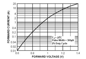
If the display screen is calibrated for voltage, one can then measure the breakdown conduction voltage of the setup to further compare the test to published data sheets, like the following one.
A resistive curve from tracking a diode
Such modern data sheets are a wealth of comparative test data. Careful comparison of each section by the curve tracer and the digital meter will provide enough data to compare each section for identical characteristics. For example, careful examination of this curve above shows the effect of the resistor in parallel with the diode.
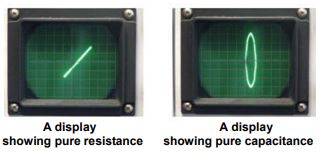
If the diode is in good condition, the visual trace will let you determine the value of the resistive and capacitive components in the stack. Note that compared to first trace at the top of this article, the “normal” one, the section which has the capacitor exhibits a linear ellipse at the point of conduction which grows more exaggerated as the capacitance is increased. The following displays show pure resistive and capacitive traces for comparison.
Displays from stacked arrays are very predictable almost to the point of forecasting a potential failure. Due to the cost of these types of stacked arrays careful documentation is warranted for future failure comparison and analysis.
As you can see, determining the condition of solid-state rectifier devices becomes easier as you go along and can see the different displays, relating them to prior tests as well as the data sheets.
Now, let us turn to an important aspect of testing high voltage rectifiers – keeping the technician safe during testing.
Safety: A Priority While Testing
High voltage stress-testing of electronic components is often one of the most helpful means of sorting the most reliable parts from the trouble-prone ones.
Hi pot (or, high potential) testing is the common name given to any type of applied dynamic voltage testing which reaches the maximum design limits and should not exceed a pre-determined value of a device.
At the same time, since we are discussing high voltage situations, it is incumbent that we also discuss personal safety.
In addition to mortality-proofing of the devices, careful hi pot testing serves an additional need: safety. The safety of the technician should be foremost in the design of any electronic or mechanical system.
Put plainly: the service and repair aspects of safety for the technician must never be compromised.
Safety around high voltage equipment, is, and – rightly so – should be the number one priority. When testing any suspect diode device, capacitor, arc gap, or reactor for any voltage parameter over 25 Volts you must remember that amperage kills, not voltage.
Indeed, just a sweaty pair of hands in the wrong place can well lead to instant cardiac arrest.
Take Care, Be Safe
One way to improve safety: when testing components for high voltage stability or intermittent arcing problems, the frame of most large devices should be suitably isolated from the technician and must be properly grounded or isolated as the device requires.
Furthermore, goggles or safety glasses should be used when stress testing any suspect device. Damaged or cracked high voltage parts will sometimes explode dangerously when stressed.
Just as with the high voltage capacitors in a transmitter, you may well run into a large reactor or other assembly that will appear normal on the outside while being electrically defective in a non-visible area. Any hi-pot testing should be done carefully to avoid over stressing any dielectric ratings specified for a particular unit.
At first look, this is a transformer that appeared normal when viewed from one side.
![]()
However, the transformer was anything but normal.
However, when inspected on the opposite site, it was clearly visibly defective – there was a hole caused by a winding that burned through, adjacent to the core frame, and gave a partial short to the unit frame. By being observant, such physical inspections can save the technician valuable diagnostic time.
Although this unit operated for some time before exhibiting erratic overload conditions, subsequent hi pot testing at elevated operating temperatures showed unsafe leakage to the grounded frame of the winding core.
Burn, Dust, or Dirt Concerns
Similar Hi Pot problems can arise from arced-over insulators for stud mount devices and open frame units. And dirt may set up an arc path that once started, may not trip or burn right away – but will certainly do so when you least expect it and seemingly for no good reason.
Many large coil wound devices also become contaminated with corona attracted dust and other semi-conductive materials. In situations of sufficiently high voltage and humidity these dirt trails will become flash and circulating current paths and possibly energize a protective cage or mount.
Because of this possibility, whenever working around high voltage, never stand on conductive floor coverings. Static drain types of flooring should always have a non-conductive kneeling mat on the standing or kneeling area.
Caution, Not Excessive Fear
Please do not become turned off by these warnings.
Especially for those who have come out of the IT areas, yes, the high voltages present in some broadcast gear can be hundreds or thousands that found in computers. Respect for this voltage is critical. But simple precautions will reduce any physical danger considerably.
For example, never wear any type of jewelry while working – and try to keep one hand free or in your pocket. A conductive path from one hand to nowhere is better than from hand to hand or foot.
Good Engineering Practices Yield Benefits
When working with a partner, common sense, clear communication, and a clear procedure might well mean “the life you save may be your own.”
Equally so, by becoming adept at test procedures as outlined above, you will not only have saved time, effort, and money, but will have improved operations at your facility.
– – –
Gary Minker is president of Radio Works RF Consulting, in Lake Worth, Florida. He can be contacted at gary@radioworksrfconsulting.com or (561) 969-9245.